 Become a TechRadar Insider


Considering one of the best motherboards is an ideal way to ensure your gaming PC's longevity without any future problems. An often overlooked component of the building process, the right board can provide your system with stable performance, ease of upgrading chipsets, and all the ports you need for not just your CPU, but your GPU, RAM, NVMe SSDs, and more.
With that said, there's no one-size-fits-all answer for the best motherboards, as there are two chipset manufacturers (AMD and Intel) with varying socket types available depending on the processor. Then there's the size of the mobo itself. Most people will be happy enough with a standard ATX for a mid-tower build, but should you want the extra headroom, you may want to consider an E-ATX instead.
Consequently, you can go the other way and build a smaller gaming PC which wouldn't be out of place under a TV in your living room or tucked away neatly on your desk. This will mean considering either a micro-ATX or a mini-ITX. These options will offer less silicon to build on at the cost of space; all major components will be covered, though. That's why you'll find all shapes and sizes below from trusted manufacturers to help you get started.
This is just the start of your building journey. Next, you'll want to consider one of the best processors, the best graphics cards, and some of the best RAM to make your system sing. We also recommend checking out the best PC cases if you're still undecided as to what chassis works for you; and if you're really stuck with where to start, then our PC building guide has you covered.
Coming to terms
Why you can trust TechRadar We spend hours testing every product or service we review, so you can be sure you're buying the best. Find out more about how we test.
If you’re unfamiliar with the best motherboards out there, use this list as a primer for your next build. Motherboards are available in a broad range of different form factors, the most common of which are ATX and Micro ATX. However, there are plenty of less common form factors including mini ITX and E-ATX. Don’t worry though, most of the best PC cases will support more than one form factor.
Moreover, in our rundown of the best motherboards, we detailed the socket type that each mobo adheres to. The socket, for those not in the know, is the part on the motherboard that the CPU locks into. Typically, newer Intel processors use either LGA 1151 or 2066 while the latest AMD Ryzen architecture is designed for the AM4 chipset.

It might not be cheap, but the Rog Maximus XIII Hero is worth its price tag. Its list of features, which includes Wi-Fi 6, PCIe 4.0, tons of ports (including two thunderbolt), and four M.2 SSD sockets, will satisfy just about anyone looking for a premium Z590 board to build a PC around. It’s not only a great performing board, but it’s easy to overclock as well. And, like any good ASUS motherboard, it comes with plenty of RGB lighting.

High-end motherboards may cost a fortune, but if you’ve got something like the MSI MEG Z490 Godlike under the hood, you’re pretty much guaranteed top-notch performance, especially if you’ve got Intel components. As long as you’re willing to pay the price. In fact, we’d go as far as to say that this is the best z490 board out there right now, with an excellent thermal solution, staggering overclocking performance, easy installation and diagnostic solutions for do-it-yourself-ers, and a solid build.

The GIGABYTE Z490 Gaming X may not have any flashy new features to bring to the table, but if you’re an Intel fan who needs a new motherboard in the budget sphere, it’s certainly a great choice. This entry-level motherboard for gamers has a decent feature set for its price tag, including three PCIe 3.0 x4 M.2 slots, six SATA ports and four memory slots with support for DDR4-4600 and up to 128GB, to start. Most importantly, it performs like the best of them without burning a hole in your pocket.

If you’re looking for a premium option for your 10th and 11th generation flagship Intel chips, the MEG Z590 Ace from MSI not only delivers a lot of power, but also comes with four M.2 sockets, two Thunderbolt USB-C ports and Wi-Fi 6E support, as well as excellent audio solution with latest premium ALC4082 audio process. There’s a lot to appreciate here, if you can afford that steep $499.
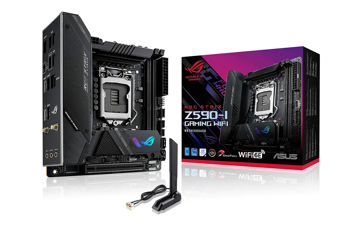
This mid to high-end Mini-ITX motherboard offering from Asus is feature-rich, with two M.2 slots, four SATA 6Gb/s ports and plenty of connectivity. In terms of design, that small form factor boasts an all-black design, diagonal mesh lines and RGB-enabled ROG logo for a fantastic aesthetic. Its performance is on point as well, delivering great network performance, excellent audio and well-balanced thermal.

If you’re considering an AMD setup for that PC you’re building, then you cannot go wrong with the ASRock X570 Phantom Gaming X. This is the best motherboard for AMD fans right now, with a top-notch feature set, great design and a highly-effective cooling solution. It’s certainly a favorite among overclockers out there, and with Wi-Fi 6 support to boot. If you have a penchant for tweak and upgrade your internals, there might be some limitations as to what you can do physically. But, other than that, it’s hard to find fault in this board.

The Gigabyte Aorus X570 Master is not only an aesthetically pleasing motherboard, with splashes of silver on a black board meant to complement its RGB lighting. It is also capable of being the centerpiece of a very powerful computer. It can handle up to 128GB of DDR4400 RAM, the latest 3rd gen AMD processors and multiple GPUs for anyone wanting to future proof their gaming needs. The X570 Master is also very astutely designed, with shielding on its I/O ports, WiFi 6 and a number of other placement choices that make this a quality board. Best of all, its price is significantly less than the high end Intel motherboards.

If you’re looking to build from scratch, the Asus ROG B550-E Gaming Motherboard is a cost-effective and feature-rich motherboard to pair with that AMD 3rd gen Ryzen chip you just bought. Its I/O ports are shielded, it comes with a PCIe 4.0 slot (and a second PCIe 3.0 one), and it has just about all the ports and port headers you could desire. With this motherboard, you’re getting excellent power delivery, a great feature set and an incredibly effective cooling solution, as well as a cool aesthetic to boot.

An upgrade from its predecessor, the B450, the Asus TUF Gaming B550M-PLUS boasts not only a much better power solution and a great cooling solution, but also game-ready features and military-grade components. Among those features are the AI Noise-Canceling Microphone software, which supports 3.5 mm, USB or Bluetooth headsets, and full RGB lighting control. All, of course, while still touting that TUF Gaming Alliance promise for easy compatibility and building, as well as aesthetics that complement its trusted partners.
To save money on Asus products, check out our Asus voucher codes.

Looking into an AMD B550 motherboard might be necessary if you’re upgrading your AMD Ryzen processor, and the NZXT N7 B550 is an excellent mid-range option. This gaming motherboard is not only designed around the B550 chipset, but it comes with built-in Wi-Fi 6E connectivity, something that you’ll be hard-pressed to find in rivalling boards. It also comes with more USB ports at the rear, making it more versatile. And, of course, you’ll also appreciate the digital RGB and fan controls through CAM.

The X-series processors are here, and they are spectacular. But if you want to take advantage of all they have to offer, you need an X-series motherboard. This ASRock X299 is an incredible choice with support for overclocked memory speeds up to 4400MHz(!!!) and 8 different slots for memory modules. It also supports up to 128GB of RAM. Add in an X-series processor and a good graphics card or 3, and this thing will absolutely tear apart anything you could possibly throw at it. If you’re seeking one of the best motherboards money can buy, this is it.

When you’ve got an AMD Threadripper under the hood of your PC, you absolutely need a beast of a motherboard like the MSI Creator TRX40. This is designed and built specifically for creators with the most demanding computing needs, this motherboard also boasts quite a feature set. Among those features are the latest PCIe gen4 slots and M.2 connectors, USB3.2 Gen2x2, Wi-Fi 6 and 10G LAN, as well as MSI’s Frozr Heatsink design and Mystic Light RGB lighting. It’s a little pricey, especially next to the competition, but then again, nothing in the creative sphere isn’t these days. If you want the best motherboard for your professional creative endeavors, it doesn’t get better than this.
Best motherboards: Frequently Asked Questions
Who makes the best motherboards?
While there's no definitive answer of the best standout manufacturer, from our testing we're confident in recommending MSI, Gigabyte, Asus, and ASRock as the big four to get you started. These brands are known for their reliable mobos and advanced feature sets.
What size motherboard is right for me?
The most conventionally sized motherboard is a Standard ATX which will be most comfortable inside a mid-tower and a full tower. However, if you want a small form factor machine, the Micro-ATX and even Mini-ITX depend on the case size. These smaller boards will have space for your CPU, RAM, NVMe SSD and other essential components, but may cut out other connectors to save on the silicon. On the reverse, you can opt for an E-ATX (or extended ATX) larger than a standard model, allowing for more room to build provided your chassis is large enough.
Does your CPU have to match your motherboard?
Yes, you must buy the correct motherboard for your processor. The most important thing is to check the socket type before purchasing. For example, if you have an AMD CPU, it will either be an AM4 or AM5 socket, and the most recent Intel processors (since 2021) have been LGA 1700 with Alder Lake (12th Gen) and Raptor Lake (13th and 14th Gen). However, if you have an older CPU, then the socket will need to match.
