From sandy beach to Kaby Lake: How sand becomes silicon
The amazing journey that ends up with a processor inside your PC
Sign up for breaking news, reviews, opinion, top tech deals, and more.
You are now subscribed
Your newsletter sign-up was successful
Join the club
Get full access to premium articles, exclusive features and a growing list of member rewards.
Step 5: Make some MOSFETS
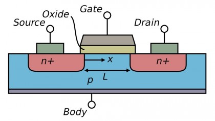
The fundamental building block of a processor is a transistor called a MOSFET, which is short for Metal Oxide Semiconductor Field Effect Transistor (although the M bit is often out of date: what was previously metal is often polycrystalline silicon).
A MOSFET is essentially a switch that is either on or off, and to make it you need to create two different regions known as p-type and n-type regions. To do that, the wafer is blasted with a beam of boron ions, positively charged boron atoms that become embedded in the silicon. The photoresist layer blocks the beams to ensure that the ions only go where they're supposed to, creating what's known as p-wells.
A second photoresist pattern is now applied, and the beam changes to phosphorous ions. These create n-wells. A more powerful phosphorous beam is then applied to create the regions that will act as the source and drain of the switches, and a pattern oxide layer is deposited before a layer of silicon-germanium doped with boron is applied. With the MOSFETs created, the next step is to make the gates that control their voltage.
Article continues below 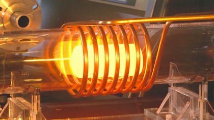
Step 6: Get the gates
A gate is an electrode that sits between the switch's source and drain, insulated by a very thin layer of metal oxide. The most recent Intel processors use second-generation Tri-gate transistors, which as the name suggests uses three-dimensional gates instead of the traditional two, and they employ a variation on MOSFETs known as FinFET or multi-gate architectures. These improvements enable Intel to drop the size of its architecture from 90nm to 22nm and even 14nm while increasing performance and efficiency.
To create a gate, a thin layer of silicon dioxide is deposited using a process called Chemical Vapour Deposition, or CVD for short. This takes place in a furnace filled with gases that cause a chemical reaction on the surface of the silicon. CVD is used again to apply a layer of silicon, this time by reacting silicon hydride gas with oxygen to produce silicon and water.
Step 7: Connect with copper
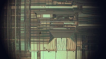
Once the gates have been created, the wafer will contain billions of MOSFETs or FinFETs, ready to be carved up into individual chips containing millions of switches. But first, the switches and gates need to be connected. That's achieved by putting down a layer of silicon oxide insulation, to ensure that the interconnecting tracks don't short out all of the switches. Once that has been applied, it's time to add the copper. One method of doing that is called the 'double Damascene', and it involves creating tungsten connecting pins and copper interconnects.
First of all, hydrofluoric acid is used to etch holes in the insulation, guided by a layer of photoresist. Then the trenches for the interconnection tracks are etched, again through a layer of photoresist. A top layer of copper is applied by electroplating, which fills the trenches and holes to make contact with the underlying switches and which creates metallic pins protruding through the insulating layer. These are known as vias. Finally, the wafer is polished to remove the excess copper, leaving only the desired tracks in the trenches and holes.
Sign up for breaking news, reviews, opinion, top tech deals, and more.
Step 8: Complete the circuit
You can't always wire up a circuit without having some wires crossing, and that's disastrous for CPUs: one rogue interconnection could make any tracks that cross it short out. To avoid this, MOSFETs have multiple metallic layers, each insulated by a layer of silicon dioxide and connected with vias.
Step 9: Throw out the bad ones
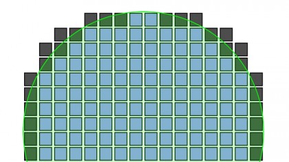
As you can probably imagine, such an incredibly complex process is prone to all kinds of potential problems, so while each wafer will contain a few hundred 'dies' – the official name for chips – many of the dies will have, er, died.
A typical yield from a wafer is around 60%, although the numbers depend on the process used – whenever a manufacturer moves to a new, more compact architecture, yields inevitably fall until production teething problems have been identified and addressed. A device called a wafer probe tests the dies, the wafer is sawn up into individual chips and the non-working ones are discarded. Slightly faulty dies may be reused as lower specification products.
Step 10: Add bubble wrap
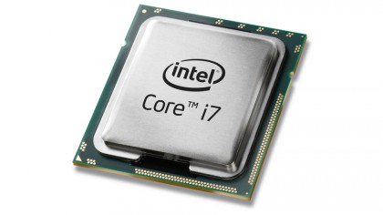
The die may be a completed processor, but it's far too fragile to ship in its current state. That's why the manufacturer then puts the bare chip in the package that we tend to visualise when we think of a processor. The die's contacts are connected to the package's contacts, and it's ready to ship and to stick into a motherboard. All that's left is some final quality assurance and the processor can begin its journey to the heart of your PC.
As a final note, fancy watching some video footage of how chips are made? The following clip is from a few years back, but it's certainly an interesting visual illustration of how Intel produces chips with 3D transistors.
Image Credit: All images used in this article are from Wikimedia
This article is part of TechRadar's Silicon Week. The world inside of our machines is changing more rapidly than ever, so we're looking to explore everything CPUs, GPUs and all other forms of the most precious metal in computing.
- Check out the current 10 top processors from AMD and Intel
 Become a TechRadar Insider


