
 Become a TechRadar Insider


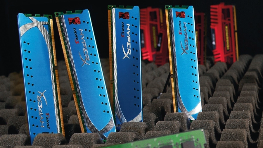
Twenty quid. That's all you need to bag a couple of memory sticks packing 4GB of RAM from one of the big brands like Crucial.
Not enough for serious multi-tasking, you say? 8GB can be had for under £40.
With decent CPUs costing north of £100, graphics cards likewise, and SSDs denting wallets across the land, thank goodness memory is cheap.
You could argue that's just as well. After all, memory has become gradually less critical to system performance in recent years, and the difference between kits has become a game of margins.
So, is it now a simple case of slapping in 8GB of any old RAM and not giving it another thought? Up to a point, yes.
Most PCs, most of the time, will do just fine with 8GB of poverty spec memory. That's enough for all but the most demanding multi-tasking scenarios.
It's sufficient to have a whole hill of browser windows open, plus a holiday's worth of high res images on the go in Photoshop, and still be able to Alt+Tab in and out of your favourite 3D frag-fest without any laggy disk swapping.
What's more, modern PC platforms are a lot less flaky when it comes to compatibility and stability. We muck about with an awful lot of kit here, and it's become rare to find memory shonky enough that it stops a rig booting.
In the basic operational sense, stuff tends to just work.

For reasons we'll come to momentarily then, modern CPUs are less dependent on memory specs and performance to deliver the goods. If that sounds like an argument for spending as little as possible, here's the counter case.
Memory still impacts system performance. Not dramatically, but if the price is only a couple of quid, it's actually one of the most cost effective ways to improve performance.
In other words, you'd be bonkers not to buy the right bits of memory. Here's how to win the game of margins.
We've established that the days when fancy memory could put a rocket up your PC's performance are long gone, but that doesn't mean memory no longer matters.
There's still plenty of opportunity to get it wrong.
What's more, with memory prices almost comically low, there's really no reason to mess things up by cutting corners. So, why isn't memory as critical as it used to be, and what do you still need to worry about?
When it comes to PC platforms, the most significant new technological trend in recent years has been the consolidation of more and more features into the CPU die. Intel, and particularly AMD are now bunging everything into CPUs.
The end game is the so-called SoC, or system on a chip, where pretty much everything of any significance is packed into a single die.

Historically, SoCs have been the weapon of choice for anything that needs to be either very cheap or very small. Think set-top boxes and mobile phones.
We're still a few years off achieving SoCs in PCs, but today's mainstream Intel CPUs, for example, pack everything from a memory controller to a PCI Express bus, and even slightly shonky graphics cores too.
The most relevant item, of course, is that memory controller. Situated on the CPU, it allows for much more memory bandwidth.
Even at entry-level memory frequencies, which means 1,333MHz right now, there's more than enough bandwidth to feed the latest multi-core processors. That applies to both AMD and Intel chips with dual-channel memory controllers. They deliver roughly 20GB/s of raw bandwidth.
As for Intel's new X79 high end platform and its quad-channel architecture, it's complete overkill.
The upshot is that you can ramp up the memory frequencies and see little or no change in overall system performance. When you already have all the bandwidth your CPU can eat, heaping on a load more doesn't make any difference.
Easy overclocking
The other change that's taken the pressure off memory involves overclocking.
In the good old days most, if not all, overclocking was achieved courtesy of cranking up bus speeds. When you do that, it has a knock on effect on all sorts of other components, including memory.
Now, it is of course true that many motherboards offered memory dividers that allowed you to scale back on memory speeds when overclocking, but really big overclocks still required fast memory, and even modest upclocks resulted in memory running at some funky non-standard speeds. But no longer.
Nearly all AMD CPUs of any interest are now unlocked. That means you have full access to the CPU multiplier and thus the ability to set core clocks without impacting other areas of the chip.
We only wish we could say the same of Intel. It still keeps most of its processors at least partially locked. Only K Series and Extreme models are unlocked.
As for the rest, from the introduction of the Sandy Bridge family of CPUs, Intel has hardlocked everything to the baseclock, so things like the PCI Express bus scale up when you tweak the baseclock.
And that has pretty much killed overclocking for locked Intel processors. They won't clock up by more than a few percentage points via the baseclock.
All of which means you don't really need fast or fancy memory for basic, default-frequency performance or as an enabler for achieving nippy overclocks.
So, does it make any difference at all, and if so, is it merely a matter of operating frequencies?
The range of performance in our World in Conflict minimum frame rate benchmark (it's minimum rather than average frame rates that really matter) was 42 frames per second at the low end right up to 50 frames per second.

Memory latency
This is where things get a little complicated.
There's more to memory than raw frequency. Memory latency – also known as memory timing – matters, too.
Typically, you'll see a set of four latency specifications quoted for any given memory kit, something along the lines of 9, 9, 9, 24.
In simple terms, the latencies represent the time in operating cycles it takes the memory to execute a certain task. It might be the number of cycles needed to send a command to the memory and receive a reply, or how many cycles you must then wait to access the memory again. Frankly, the details don't matter much.
"Like clockspeeds, memory latencies can be tuned"
All you really need to know is that the lower the numbers, the better it is for performance. Indeed, really poor latency can be more of a drag on performance than mediocre operating frequencies.
And here's the kicker: when you increase memory clockspeeds, the latencies go up. It can be a bit of a zero sum game with today's bandwidth-saturated CPUs.
Of course, just like clockspeeds, latencies can be tuned. The problem is, with at least four settings on offer, this can be fiendishly complicated. There is, however, a solution.
XMP (or Extreme Memory Profiles) is a standard cooked up by Intel to simplify memory overclocking. Essentially, it enables guaranteed memory overclocking with set latencies.
With XMP enabled, you can be confident you're getting the best, or at least very close the best, out of your memory subsystem.
There's not too much else to worry about. We're not convinced that cooling is a major issue for today's low-voltage memory, for instance.
We're happy to see some cooling fins if they don't push the price up too much, and aren't so big they compete with the CPU cooler for space inside your PC.