
 Become a TechRadar Insider


Note: Our sand to silicon chips feature has been fully updated. This article was first published in May 2009.
Strange things happen in forests – especially Silicon Forest, as Hillsboro in Oregon has come to be known. That's where D1X, Intel's largest operational fabrication plant, is based – and it's where what would have once seemed like a miracle of engineering is performed all day every day.
Article continues below- Also check out: 10 CPUs that changed computing

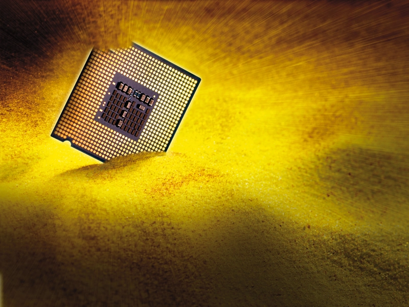
Step one: Get some sand
As you've probably guessed, chipmakers don't head for the nearest beach with JCBs or place bulk orders with the local builders' merchant. Normal sand and the sand used in the building industry is usually coloured red, yellow or orange due to the presence of impurities. What chipmakers need is silica sand, which you usually get from quarrying.
Silica sand is also known as silicon dioxide, and as you've no doubt guessed from the name it's a compound of silicon and oxygen. To get the silicon, the oxygen is removed by mixing it with carbon and heating it in an electric arc furnace to temperatures beyond 2,000 degrees C. At those temperatures the carbon reacts with the oxygen, becoming carbon dioxide and leaving pure silicon in the bottom of the furnace. That silicon is then treated with oxygen to remove impurities such as calcium or aluminium, leaving what's known as metallurgical grade silicon. That's up to 99% pure.
Unfortunately for the chipmakers, that still isn't pure enough to meet the requirements of microscopic microprocessors. So the metallurgical grade silicon is refined further, this time by grinding it into a fine powder, adding hydrogen chloride and heating it in a fluidised bed reactor at 300 degrees C. This creates a liquid silicon compound called tricholrosilane, and it also creates chlorides of unwanted elements such as iron, aluminium, boron and phosphorus. These are removed by fractional distillation and the trichlorosilane is vaporised in hydrogen at 1,000 degrees C. An electrically heated, ultra-pure silicon rod collects the silicon, and the result is electronic-grade silicon. Its purity: 99.999999%.
It turns out that this was the easy bit.

Step 2: Make some crystals
Electronic-grade silicon still isn't perfect, because it has a polycrystalline structure. That means it's composed of lots of small silicon crystals, and the joins between those crystals can suffer from defects known as grain boundaries. Those boundaries can cause chaos with electronic signals, so the structure of the silicon has to be changed.
The process of doing that is called the Czochralski Process, and it involves melting the silicon crystal in a quartz crucible at just over the melting point of 1,414 degrees C. A tiny silicon crystal is then dipped into the molten silicon, and it's drawn out while rotating constantly in the opposite direction to the rotation of the crucible. This attracts silicon from the crucible, creating what's known as a boule. A boule is a rod made from a single silicon crystal, and its size depends on the temperature, the rate of spin and the rate at which the crystal is pulled from the liquid. A typical boule will be around 300mm across.

Step 3: Cut your wafers
The circular silicon rod is now cut into wafers, and those wafers are cut as thin as possible without making them incapable of surviving the fabrication process. The rod is cut with a device that works rather like an egg slicer, cutting multiple slices simultaneously to create wafers 0.775mm thick. The wire constantly moves and carries a slurry of silicon carbide, the same abrasive material that's used to make wet and dry sandpaper. The sharp edges of the wafers are then smoothed to prevent them from chipping.
Next up: lapping, where the wafers' surfaces are polished using an abrasive slurry until the wafers are flat to a tolerance of two thousandths of a millimetre. After that, the wafer is etched with a mixture of nitric, hydrofluoric and acetic acids to create an even smoother surface.

Step 4: Make patterns
The super-smooth wafers will now be given an oxide layer, which is used to create the required features of the circuit. This is done selectively to specific areas, and may involve the use of ion beams, hot gases and/or chemicals.
Once such chemical is known as "photoresist", and it's broadly similar to the chemicals used to make photographic film. Unfortunately that doesn't cope very well with hot gas treatments, so the wafer needs to be masked. This is done by applying a patterned oxide layer that ensures the gases don't reach the photoresisted bits that the chip designer wants to keep.
There can be up to six steps in this process:
- The wafer is heated to a high temperature in a furnace, creating a layer of silicon dioxide as the silicon reacts with oxygen
- A layer of photoresist is applied, with the wafer spun in a vacuum to ensure even coverage and then baked dry
- The wafer is exposed to UV light through a photographic mask or film, once for each chip or cluster of chips on the wafer. The wafer is moved between each exposure using a machine called a 'stepper'
- An alkaline solution is applied, dissolving the sections of photoresist that were exposed to the UV light. Those sections are washed away
- Hydroflouric acid is used to dissolve the parts of the oxide layer where the photoresist has been washed away
- A solvent is applied to remove the remaining photoresist, leaving a patterned oxide layer in the shape of the required circuit features