Intel CEO teases with 22nm silicon
Otellini claims 'working chips', with more powerful processors to come

Sign up for breaking news, reviews, opinion, top tech deals, and more.
You are now subscribed
Your newsletter sign-up was successful
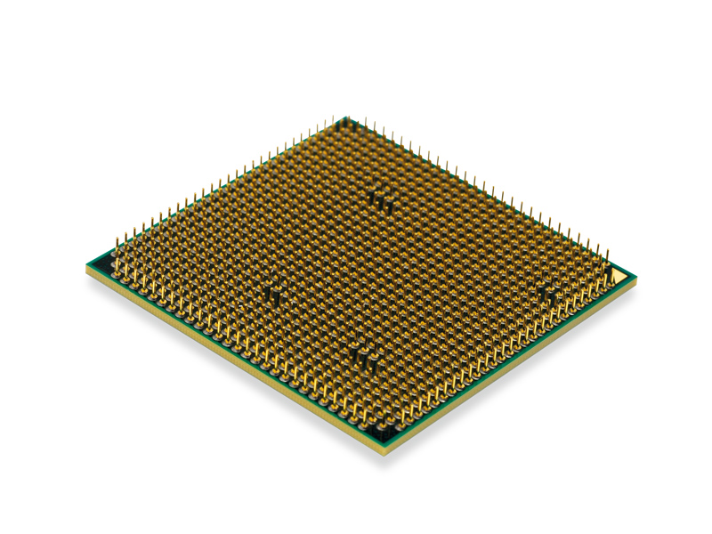
Intel President and CEO Paul Otellini today displayed a silicon wafer containing the world's first working chips built on 22nm process technology.
The 22nm wafer on show at the Intel Developer Forum in San Francisco is made up of individual die containing 364 million bits of SRAM memory.
The chip contains more than 2.9 billion transistors packed into an area the size of a fingernail.
Article continues belowLess is Moore
"At Intel, Moore's Law is alive and thriving," said Otellini. "We're already moving ahead with development of our 22nm manufacturing technology and have built working chips that will pave the way for production of still more powerful and more capable processors."
Otellini also confirmed that 32nm microprocessors were in full production, the first processor to integrate graphics with the CPU. Following the move to 32nm, Intel will introduce Sandy Bridge, Intel's next new microarchitecture. Sandy Bridge will feature a sixth generation graphics core on the same die as the processor core and includes instructions for floating point, media, and processor-intensive software.
Also showcased at the Forum was Intel's Moblin (Mobile Linux) operating system for Atom-based MIDs and mobile phones, which is now up to version 2.1. The new OS has been optimised for smaller phone screens, with a panel-based navigation system.
Sign up for breaking news, reviews, opinion, top tech deals, and more.