MIT breakthrough means your next computer could be even thinner and flexible too
Chip production breakthrough uses different materials in the same layer

Sign up for breaking news, reviews, opinion, top tech deals, and more.
You are now subscribed
Your newsletter sign-up was successful
Join the club
Get full access to premium articles, exclusive features and a growing list of member rewards.
It's impressive to see how thin some laptops have become these days, but that's nothing compared to the ultra-thin machines of the future – which may be closer to reality thanks to a new chip production breakthrough from MIT (Massachusetts Institute of Technology).
Whereas today's computer chips are produced by stacking separate layers of different materials, the breakthrough from MIT researchers (documented in the publication 'Advanced Materials') has seen different materials used in the same layer for the first time.
This is a wholly different way of operating, and the resulting experimental chips which have been produced – and working chips have been made with all components necessary to have a functioning general-purpose computer – are extremely thin indeed.
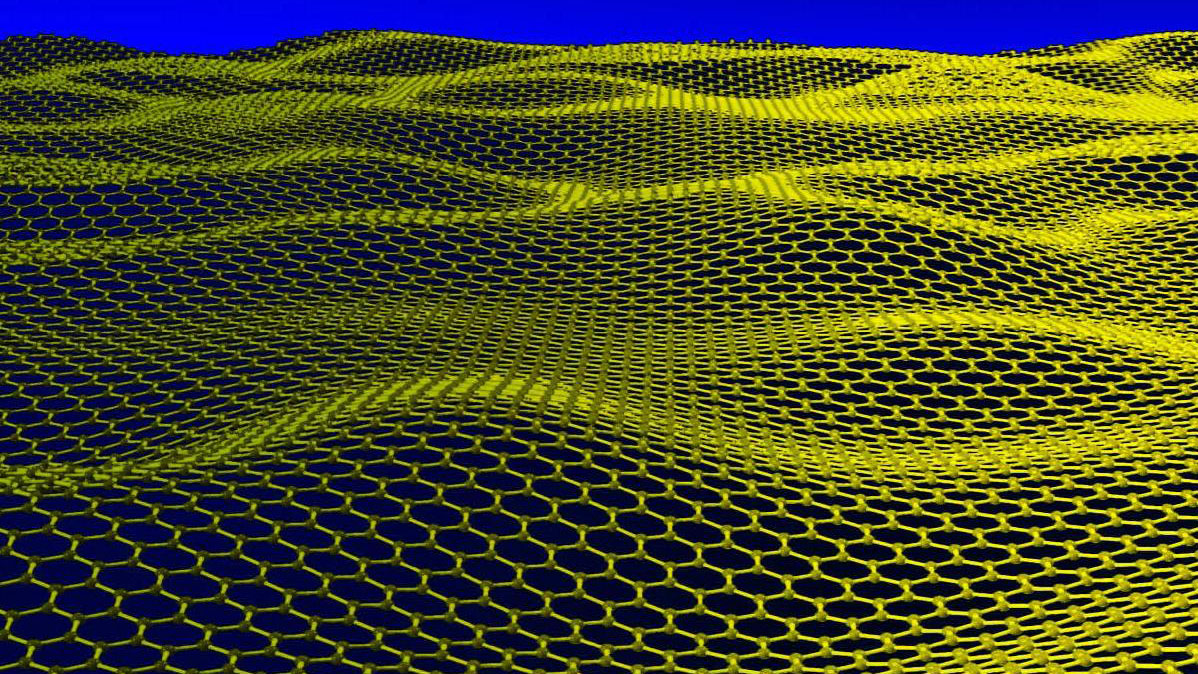
Article continues belowAs MIT News reports, we are talking between one and three atoms thick, and such components in turn will mean incredibly thin and indeed flexible computing devices.
While all manner of elements could potentially be used, the experimental chip the researchers worked with employed two materials, namely molybdenum disulfide and graphene (the latter has long been thought of as being at the heart of the next major computing breakthrough in terms of pushing hardware to its limits).
Turbo-tunnelling
This isn't just about thin and light, but the new fab method could also help push forward the development of tunnelling-transistor processors which would mean a major leap in terms of pure computing power.
Tunnelling-transistor tech involves, and we quote, a "counterintuitive quantum-mechanical effect". Where a standard transistor either allows a charge to cross or not, with a tunnelling-transistor, an electron effectively disappears at one location and reappears at another.
Sign up for breaking news, reviews, opinion, top tech deals, and more.
Because they work in this way, tunnelling-transistors aren't bound by the same thermal inefficiencies as traditional transistors, and so in a nutshell, they can operate extremely efficiently achieving much higher speeds.
Philip Kim, a professor of physics at Harvard University, commented: "This work is very exciting. The MIT team demonstrated that controlled stitching of two completely different, atomically thin 2D materials is possible. The electrical properties of the resulting lateral heterostructures are very impressive."
As ever, though, super-thin and bendy computers are a long way down the road, but they may just have moved that much closer.
- Also check out: How graphene could revolutionise the tech industry
Darren is a freelancer writing news and features for TechRadar (and occasionally T3) across a broad range of computing topics including CPUs, GPUs, various other hardware, VPNs, antivirus and more. He has written about tech for the best part of three decades, and writes books in his spare time (his debut novel - 'I Know What You Did Last Supper' - was published by Hachette UK in 2013).
 Become a TechRadar Insider


