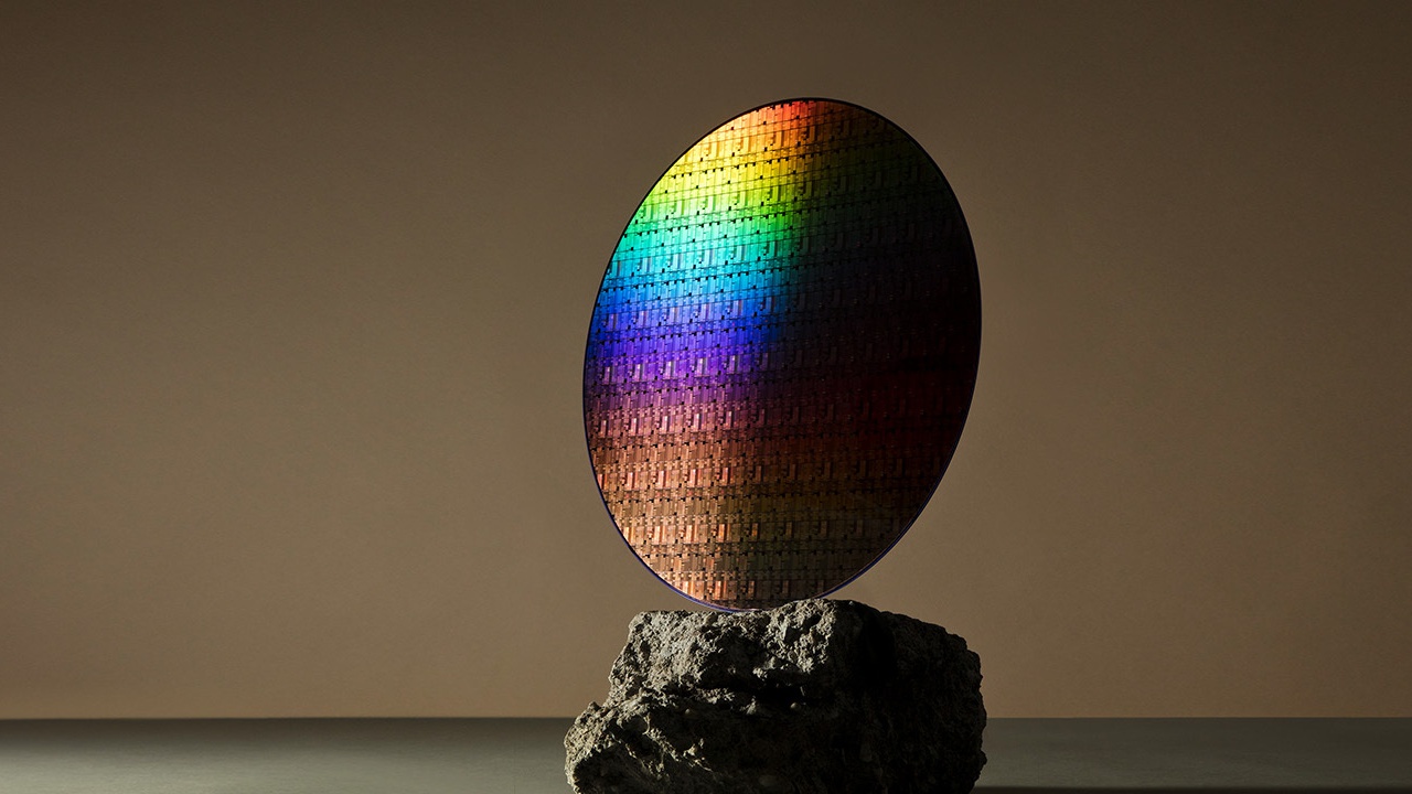
IBM, Samsung claim breakthrough in chip design: charge your phones once a week
"A huge leap forward"

Sign up for breaking news, reviews, opinion, top tech deals, and more.
You are now subscribed
Your newsletter sign-up was successful
Smartphone batteries losing juice is the perennial plaint of most users. Despite many strides being made on battery technology, a breakthrough is still elusive. But, as it happens, tech majors IBM and Samsung are now jointly claiming a major advancement in semiconductor design that can eventually lead to "cell phone batteries lasting a week without being charged.
Cutting to the chase, IBM and Samsung has been working to stack up semiconductor transistors vertically to free up more space on the silicon. The research apparently has resulted in them creating VTFET, a new kind of transistor that can be more densely packed onto a computer chip (as opposed to the conventional FinFET transistor.)
For the record, VTFET is Vertical Transport Field Effect Transistor while FinFET is Fin field-effect transistor. The new technology has been developed at the Albany Nanotech Complex in New York, which is home to a world-leading ecosystem of semiconductor research and prototyping.
Article continues below- Is the future of processors already here?
- IBM has made the first 2nm processor, but don't expect a 2nm gaming CPU soon
What is this VTFT technology?
Basically, what the two companies have done is instead of attaching transistors on a semiconductor that lie flat, they have built the transistors vertically on the chip surface, allowing a vertical current flow and allowing more transistors on a given surface. It is well known that more transistors mean that more calculations can be processed per second.
Analysts liken the change to building a high-rise structure as against a single floor design that the previous tech represented.
The VTFET approach also creates more contact points for transistors for greater energy flow and lower waste. In addition to a reduction in energy usage, the new design means two times the performance of finFET chips.
"At these advanced nodes, VTFET could be used to provide two times the performance or up to 85% reduction in energy use compared to the scaled finFET alternative," IBM said in a statement.
Sign up for breaking news, reviews, opinion, top tech deals, and more.
Less energy and more efficiency
"We believe that the VTFET design represents a huge leap forward toward building next-generation transistors that will enable a trend of smaller, more powerful and energy-efficient devices in the years to come," IBM said.
If this indeed makes it to mainline market on actual consumer chips, apart from improved cellphone batteries that last for a week, energy intensive processes, such as cryptomining operations and data encryption, "could require significantly less energy and have a smaller carbon footprint".
The lower energy needs can also help in expansion of IoT and edge devices and help them operate in ocean buoys, autonomous vehicles, and spacecraft.
The companies didn't say when the VTFET technology will arrive as an official chip manufacturing process. But the two companies announced that Samsung will manufacture IBM chips at 5 nm node to be used in IBM server platforms. In 2018, they announced Samsung would make 7 nm chips for IBM used in IBM’s Power 10 servers released earlier in 2021.
The IBM Telum processor is also made by Samsung. Recently, IBM announced the 2 nm chip technology breakthrough which will allow a chip to fit up to 50 billion transistors in a space the size of a fingernail.
All said, the new tech is challenging the famed Moore's Law --- the principle that the number of transistors incorporated in a densely populated IC chip will approximately double every two years. In the future engineers may run out of space to cram in more transistors. But till then, technology will keep giving.
Want to know about the latest happenings in tech? Follow TechRadar India on Twitter, Facebook and Instagram

Over three decades as a journalist covering current affairs, politics, sports and now technology. Former Editor of News Today, writer of humour columns across publications and a hardcore cricket and cinema enthusiast. He writes about technology trends and suggest movies and shows to watch on OTT platforms.