Entering the third dimension has huge implications for a PC's display system, but it doesn't end with a high performance graphics card and a stereoscopic monitor. 3D images put great demands on the processor and its associated memory, and storing 3D content requires vast amounts of hard drive space.
It therefore seems appropriate that a major strand in current research is improving performance by making the components themselves three-dimensional in structure.
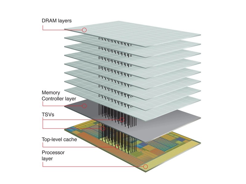
Article continues belowMulti-layered chips

PROTOTYPE CHIPS: IBM sandwiched cooling layers with water channels no wider than a human hair between layers of transistors
To see how this works, we spoke to Dr Bruno Michel, manager of Advanced Thermal Packaging at IBM Research in Zurich. "The main benefit of adopting a 3D structure is that the distances for information transport become far shorter than with 2D chips," he says.
"The second benefit is that more interconnects are possible, which further improves communication speed. The main problem of a current processor is that it takes on average 1,300 clock cycles for information to arrive from the main memory, which is some 20-30 cm away. This is partially alleviated by introducing cache memory on the processor chip, but during a 'cache miss', waiting is inevitable. In 3D chip stacks, cache memories can be much larger which reduces the waiting time and thereby considerably improves the overall efficiency."
None of this comes without some considerable challenges, the first of which is making those connections between the layers of transistors.
One method is to extend the layer-upon-layer fabrication method used today to create multiple layers of transistors with the necessary interconnections running both horizontally and vertically. This is called the monolithic approach.
Success here has been limited though, partly because the heat needed to create a new layer of transistors is often enough to destroy any connective pathways already in place. Although monolithic 3D chips could offer much greater connectivity, most of today's research has therefore been into methods of creating inter-layer connections between several wafers or dies that have been manufactured conventionally. Even this isn't without its challenges, as Dr Michel explains:
"The problem is tackled in several stages: The first is the development of the Through Silicon Via (TSV) technology, which allows chips to be stacked with short interconnect distances. This can be applied to systems that are composed of heterogeneous technologies with one chip being logic and other chips being cache memory".
In a similar vein, other researchers refer to stacking cores as a means of improving core-to-core communications.
Keeping cool
Dr Michel's second point isn't a new one, although a 3D structure exacerbates it. "The second development is the cooling technology needed, since stacking of logic chips multiplies the heat fluxes and thermal resistances with the number of layers. For this reason interlayer cooling will become mandatory when more than three processors are stacked."
IBM is addressing this issue by implementing water-cooling on a miniature scale. It has used cooling channels as thin as a human hair between the individual layers to achieve up to 180W of cooling per square centimetre on each layer.