
 Become a TechRadar Insider


Modern hyperscale datacenters have infinite appetite for storage performance, capacity, and density, which is why multiple new SSD form-factors designed to maximize performance and capacity were introduced in the recent years.
But Kioxia believes that there is a faster and cheaper way to deliver desired solid-state storage solutions to cloud customers: wafer-level SSDs.
With capacities starting at around 50 TBs using current 3D QLC NAND, such devices could offer unbeatable performance.
- Need something portable? Check out the best portable SSD
- We've also put together a list of the best M.2 SSD
- Looking to save a buck? These are the best cheap SSDs
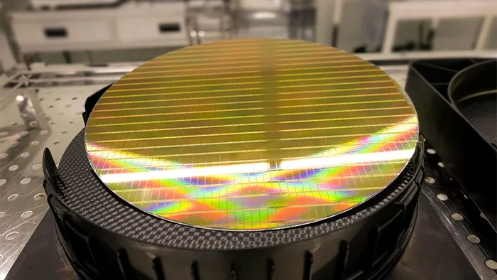
Wafer-level SSDs
In a nutshell, Kioxia proposes to skip dicing, assembly, chip packaging, and SSD drive assembly, but use a whole wafer with 3D NAND instead.
The wafer is to be probed using Kioxia’s ‘super multi-probing technology’ to discover as well as disable faulty 3D NAND dies and then attached to a pad with I/O and power connectors. The whole thing should be operated in parallel to extract maximum sequential and random IOPS performance.
The current capacity of SSDs is limited by form-factors and chip packaging technologies, whereas performance boundaries are defined by controllers (i.e., by the number of their NAND channels as well as their ability to effectively perform ECC and other necessary operations quickly) and the PCI Express interface.
On a wafer level, one can get an extreme number of NAND channels (think well beyond Microsemi’s 32 channels common on enterprise-grade SSDs), whereas a PCIe 6.0 x16 interface would deliver up to 128 GB/s of bandwidth. As for IOPS, we are talking about a multi-channel monstrous SSDs, so think of millions of IOPS.

Shigeo Oshima, Kioxia’s chief engineer, described the concept of wafer-level SSDs in a presentation at VLSI Symposium 2020, meaning this is not a product from the company’s roadmap, but hopefully something to come soon.
However Kioxia currently produces 1.33 Tb 96-layer 3D QLC NAND chips that measure 158.4 mm2 and deliver up to a 132 MB/s write performance due to a quad-plane architecture. Approximately 355 of such dies fit on a 300-mm wafer, so assuming a yield rate of approximately 90%, Toshiba gets around 320 good dies, or 53 TB of raw 3D QLC NAND. With future iterations, Toshiba will have even more raw 3D NAND per wafer.
A solid-state storage solution based on 300-mm 3D NAND wafer(s) would look like a standard rack server with its own logic, PSU, cooling system, and other components like network interfaces. From storage density point of view, such a server is not going to be a champion (not in a world where you can pack 100 TB into a 3.5-inch form-factor), but if you need extreme performance at a relatively low price, a device of such kind could make sense.
- Also check out our complete list of the best business laptops: top devices for working from home, SMB and more
Via Blocks & Files