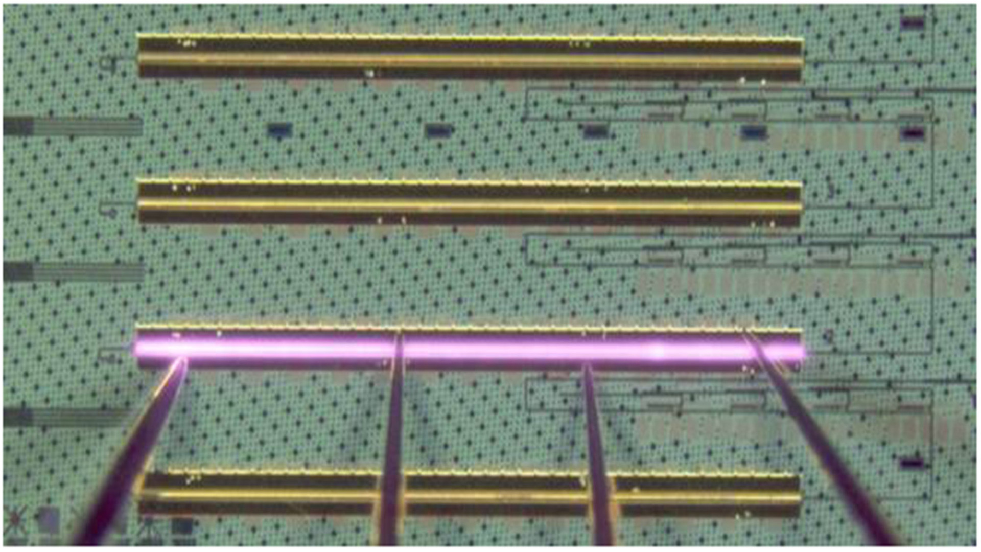
A new trick for merging lasers with silicon could finally make photonic chips cheap, fast, and ready for mass production
Quantum lasers run in the O-band, ideal for data centers and high-speed storage

Sign up to the TechRadar Pro newsletter to get all the top news, opinion, features and guidance your business needs to succeed!
You are now subscribed
Your newsletter sign-up was successful
Join the club
Get full access to premium articles, exclusive features and a growing list of member rewards.
- Photonic chips with quantum lasers are finally being built without redesigning the whole system
- These lasers work directly on silicon and still survive high heat for over six years
- University of California researchers filled the laser gap with polymers and nailed precision beam control on-chip
A new fabrication method could make photonic circuits cheaper and more practical by directly integrating quantum dot (QD) lasers onto silicon chips, a process that could influence how future smart home devices, fitness trackers, and even laptops are engineered.
The research team, led by Rosalyn Koscica at the University of California, achieved this by combining three key strategies.
They used a pocket laser configuration for direct integration, followed a two-step growth method involving metalorganic chemical vapor deposition and molecular beam epitaxy, and introduced a polymer gap-filling technique to reduce optical beam spread.
Article continues belowClosing the gap with careful engineering
This development addresses longstanding challenges involving material incompatibilities and coupling inefficiencies that have historically limited the performance and scalability of integrated photonic systems.
The combined efforts minimized the initial interface gap and made it possible for lasers to function reliably on silicon photonic chiplets.
As the researchers note, “Photonic integrated circuit (PIC) applications call for on-chip light sources with a small device footprint to permit denser component integration.”
The new approach enables stable single-mode lasing at the O-band frequency, which is well-suited for data communications in data centers and cloud storage systems.
Sign up to the TechRadar Pro newsletter to get all the top news, opinion, features and guidance your business needs to succeed!
By integrating the lasers directly with ring resonators made of silicon or using distributed Bragg reflectors from silicon nitride, the team has also addressed issues related to alignment and optical feedback.
One of the more surprising findings from the research is how well the lasers perform under heat.
“Our integrated QD lasers demonstrated a high temperature lasing up to 105 °C and a life span of 6.2 years while operating at a temperature of 35 °C,” says Ms. Koscica.
These performance metrics suggest a level of thermal stability previously difficult to achieve with monolithically integrated designs.
This thermal resilience opens the door to more durable applications in real-world environments, where temperature fluctuations can limit the reliability of photonic components.
It may also reduce the need for active cooling, which has traditionally added cost and complexity to past designs.
Beyond performance, the integration method appears well suited to large-scale manufacturing.
Because the technique can be executed in standard semiconductor foundries and does not require major changes to the underlying chip architecture, it holds promise for broader adoption.
The researchers argue that the method is “cost-effective” and “can work for a range of photonic integrated chip designs without needing extensive or complex modifications.”
That said, the approach will likely face scrutiny regarding consistency across large wafers and compatibility with commercial photonic systems.
Also, success in controlled lab environments does not guarantee seamless deployment in mass manufacturing settings.
Still, the combination of a compact laser design, compatibility with conventional processes, and integration of O-band functionality makes this development notable.
From data centers to advanced sensors, this silicon-compatible laser integration could bring photonic circuits closer to mass-market viability.
Via IEEE
You might also like
- These are the best cloud computing services available right now
- We've rounded up the best cloud hosting providers for your needs
- AMD ThreadRipper PRO 9995WX could sell for $13,000, over 2x the price of the 96-core EPYC 9655

Efosa has been writing about technology for over 7 years, initially driven by curiosity but now fueled by a strong passion for the field. He holds both a Master's and a PhD in sciences, which provided him with a solid foundation in analytical thinking.
You must confirm your public display name before commenting
Please logout and then login again, you will then be prompted to enter your display name.
 Become a TechRadar Insider


