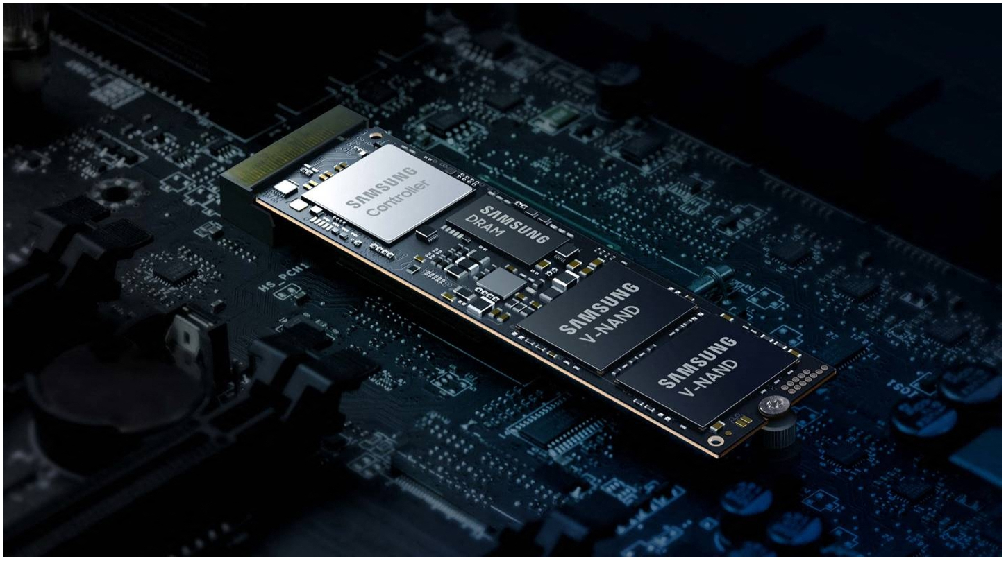
Samsung reveals more details about how it plans to produce 1000-layer QLC NAND chip that are vital for a Petabyte SSD — hafnia ferroelectrics identified as key ingredient to ramp layer count beyond 1K
We may find out more at upcoming tech symposium

It’s no secret that the race is on to produce the first 1000TB SSD. At its Tech Day in 2022, Samsung revealed ambitious plans to “stack over 1,000 layers” in its most advanced NAND chip by 2030, meaning a petabyte SSD could arrive by then.
Last year the company dropped hits that it might be in a position to deliver it much sooner, but that looks to have been wishful thinking on the tech industry’s behalf.
That said, it’s clearly full steam ahead on the development of future NAND chips. The South Korean electronics giant recently announced it would commence mass production of its newest 290-layer ninth-generation vertical (V9) NAND chips shortly, and it’s widely expected it will reveal a staggering 430-layer tenth-generation (V10) NAND chip next year.
Hafnia Ferroelectrics
So while we don’t know much about what’s going on behind the scenes in the company’s quest to produce the first Petabyte SSD, some clues have appeared online.
At this year’s VLSI Technology Symposium in Honolulu, there’s going to be a Technical Session presented by Giwuk Kim, a Ph.D student at the department of Electrical Engineering at the Korea Advanced Institute of Science and Technology (KAIST). His research interests include hafnia-based FE-NAND memory, FeRAM, and In-memory computing application, and this will be the focus of the session, which is titled “In-depth Analysis of the Hafnia Ferroelectrics as a Key Enabler for Low Voltage & QLC 3D VNAND Beyond 1K Layer Experimental Demonstration and Modeling.”
The summary of the work which – spoiler alert – has been co-authored by Samsung Electronics, reads as follows: “We experimentally demonstrate a remarkable performance improvement, boosted by the interaction of charge trapping & ferroelectric (FE) switching effects in metal-band engineered gate interlayer (BE-G.IL)-FE-channel interlayer (Ch.IL)-Si (MIFIS) FeFET. The MIFIS with BE-G.IL (BE-MIFIS) facilitates the maximized ‘positive feedback’ (Posi. FB.) of dual effects, leading to low operation voltage (VPGM/VERS: +17/-15 V), a wide memory window (MW: 10.5 V) and negligible disturb at a biased voltage of 9 V. Furthermore, our proposed model verifies that the performance enhancement of the BE-MIFIS FeFET is attributed to the intensified posi. FB. This work proves that the hafnia FE can play as a key enabler in extending the technology development of 3D VNAND, which is currently approaching a state of stagnation.”
Quite what role Samsung will play in the demonstration (if anything) isn’t known at the moment, but the firm isn't alone in exploring the potential of hafnia ferroelectrics. Giwuk Kim’s talk is part of a parent session at the symposium titled “Non-Volatile Memory Technology - Hafnia Based Ferroelectrics-1” which will be chaired by Deoksin Kil, Head of Material Development at Samsung’s archrival SK hynix.
Sign up to the TechRadar Pro newsletter to get all the top news, opinion, features and guidance your business needs to succeed!
More from TechRadar Pro

Wayne Williams is a freelancer writing news for TechRadar Pro. He has been writing about computers, technology, and the web for 30 years. In that time he wrote for most of the UK’s PC magazines, and launched, edited and published a number of them too.

 Become a TechRadar Insider


