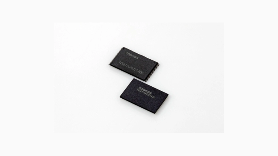
Following Intel's and Samsung's flash storage announcements, it's now Sandisk's and Toshiba's turn to announce details of their 3D NAND chips, known as BiCS. Pilot production for BiCS will kick off in the second half of 2015.
"We utilised our first generation 3D NAND technology as a learning vehicle, enabling us to develop our commercial second generation 3D NAND, which we believe will deliver compelling storage solutions for our customers," said Dr. Siva Sivaram, executive VP of memory technology at SanDisk.
Article continues belowDedicated plant being built
Intel and Micron, and Samsung have both already announced separate 3D NAND offerings, although they only used 32-layer designs. In that sense, they are already a couple of steps behind the Toshiba and SanDisk partnership. Intel, in particular, claimed that 75% of a terabyte can fit in a fingertip-sized package in its 3D NAND memory and thus lead to speculation that 10TB SSDs will become a reality.
SanDisk plans to employ the 3D NAND technology across a range of solutions, from removable products to enterprise SSDs. SanDisk expects to see commercial production kick off in 2016 at a site specifically built for 3D flash production.