
 Become a TechRadar Insider


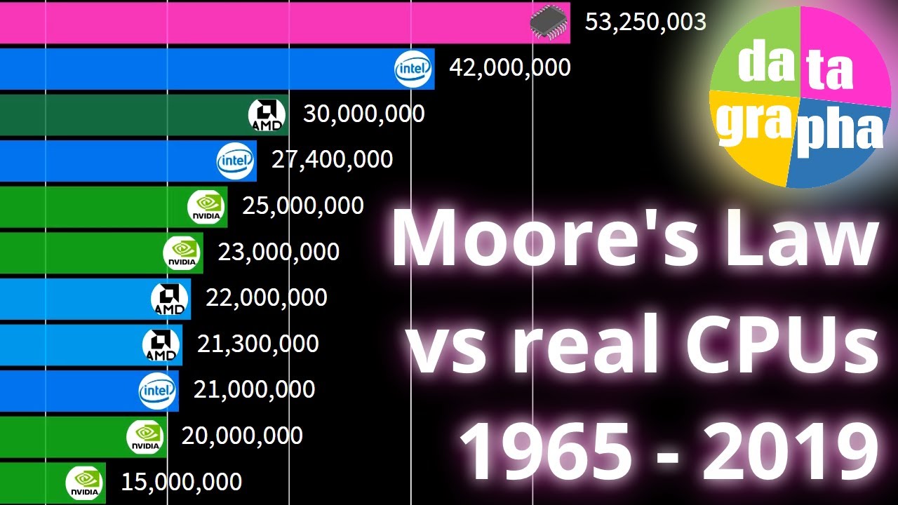
When technologist Gordon Moore predicted six decades ago that the number of transistors on a chip would double with every year, it surely occurred to no one that his calculation might carry into the next millennium.
Admittedly, the prediction was later revised to a doubling of transistor count every two years. But approximately, advances in semiconductor design have propelled Moore’s Law into the present day, delivering on the promise of a near exponential increase in processor performance.
In 1965, when the paper containing Moore’s prediction was first published, integrated circuits featured fewer than 50 transistors. Today, the most advanced system-on-chips (SoCs) house in excess of 100 billion transistors, separated by a handful of nanometers.
However, the limitations of physics mean there is only so much smaller transistors can become and only so much closer manufacturers can pack them together and still reap material rewards.
To continue to push the limits of performance beyond Moore’s Law, therefore, new methodologies will need to be explored, beyond the shrinkage of components.
One option under investigation is to place special materials in thin layers on top of silicon, the foundational ingredient of microprocessors. A few potential candidates have emerged, but one in particular is beginning to attract the attention of foundries and chip designers alike: graphene.
More than Moore
Graphene is a close relative of graphite, the material from which pencil lead is made. Whereas graphite is comprised of many layers of carbon stacked atop one another, graphene is a crystalline structure made up of just a single layer of carbon atoms. Put another way, it’s two-dimensional (2D).
Inevitably, the manufacturing of a material made up of a single layer of atoms is a delicate process (it is more accurate to say graphene is grown, by a process of crystallization). But as the material’s potential becomes better understood, more investment is being pumped into the market.
Applied Nanolayers (ANL), one of few companies able to manufacture graphene at wafer scale, identified early on that 2D materials could play an important role in overcoming the physical barriers that are soon to stop Moore’s Law in its tracks.
Paul Hedges, the company’s co-founder and CEO, says Moore’s Law will begin to falter beyond the 3nm process nodes currently in development at companies including TSMC, Samsung and Intel.

Beyond this threshold, further shrinkage becomes impractical, cooling becomes an issue and performance stagnates as a result, which means novel techniques need to be discovered and implemented. This quest is known informally as “More than Moore”.
“When scaling silicon-based transistors beyond 3nm they will suffer short-channel effects that reduce transistor performance. Transistors made from semiconducting 2D materials do not suffer from these short-channel effects and thus have the potential of extending the industry scaling roadmap,” explained Hedges.
“In the ‘80s and ‘90s, it was about developing smaller features to make chips go faster. But what’s happened since is about bringing more of the elemental table into chip fabs. Graphene is just the first of several two-dimensional materials that will enable a new class of devices to be made.”
Modest beginnings
For all its promise, graphene is currently being applied in only a small number of contexts. In these early stages, the focus is on developing new applications and designing the first few chips augmented by 2D materials.
The first graphene-powered semiconductors will support a range of IoT use cases, which stand to benefit from the material’s unique selection of properties: extreme strength, high conductivity, transparency and flexibility.
“With any new material, you have to go to wherever it will have the greatest benefit,” Hedges told us. “Currently our customers are using graphene for sensors, and photonic switching and modulators.”
“This one atom sheet is only surface, no bulk, so when a reaction takes place it is only on that very thin layer and can be measured by the changing sensitivity of the electrons passing through the graphene. This makes for very sensitive biosensors. In the case of modulators it is the high mobility and electro-optical properties of the graphene that allow for fast modulation of light.”

In addition to supplying the material, Applied Nanolayers is working hand-in-hand with early adopters in the biosensing and photonics space to develop prototypes and prepare devices for engineering at scale. By providing consultancy services as part of the application development process, the company hopes to accelerate adoption and make strongholds of these niche areas.
However, as awareness of its potential increases and the hunt for performance gains becomes ever-more urgent, Hedges expects graphene to be incorporated into general purpose CPUs and GPUs too.
“Graphene and other 2D materials will start in IoT devices and will eventually be used in switching and compute,” he said.
“Initially, graphene will be used for sensing and switching at the back end of the line (BEOL) - the last layer of the chip. Eventually, semiconducting 2D materials will form the switching devices at the front end of the line (FEOL), enhancing the silicon device structure and performance.”
Until now, the likes of Intel and AMD have been able to churn out new generations of processor on an almost yearly basis, with each offering material improvements in performance. But rubbing up against the limits of Moore’s Law, designers will have to get creative.
The foundries come calling
To his credit, Hedges was careful not to overstate the significance of the developments in the graphene industry in these early stages. “To put a knife in the hype,” he said, “[using graphene to augment silicon] is something that will only happen a little further down the line.”
One of the reasons it’s natural to start at the BEOL is that Applied Nanolayers can piggyback on mature technology, already being used in high volumes to make billions of semiconductors.
Separately, the graphene supply chain is not yet mature enough to provide the material at scale and to the necessary level of quality, a non-trivial speed bump on the road to mass adoption.
That said, there are signs that players outside the niche markets are beginning to pay close attention to developments in the graphene space, Hedges told us.
“The first ten years got us to the point at which the technology is being deployed; early customers are a mixture of new companies and corporates [across the IoT space],” he said. “But we’re also increasingly dealing with chip foundries. They have customers who need these materials too, so they’re asking about supply of materials and help with integration.”
Applied Nanolayers is already in conversation with two “major fabs” (Hedges was unable to supply the specifics), but broadly the objective is to be primed and ready when the largest players in the industry come looking for a way to bring More than Moore to fruition.
- Our list of the best workstations on the market today
