


Dutch lithography machine manufacturer ASML recently dethroned Applied Materials to become the world's largest fab tool maker, and its future looks even brighter following the news that it is gearing up production of its new High-NA (numerical aperture) EUV (extreme ultraviolet) machine.
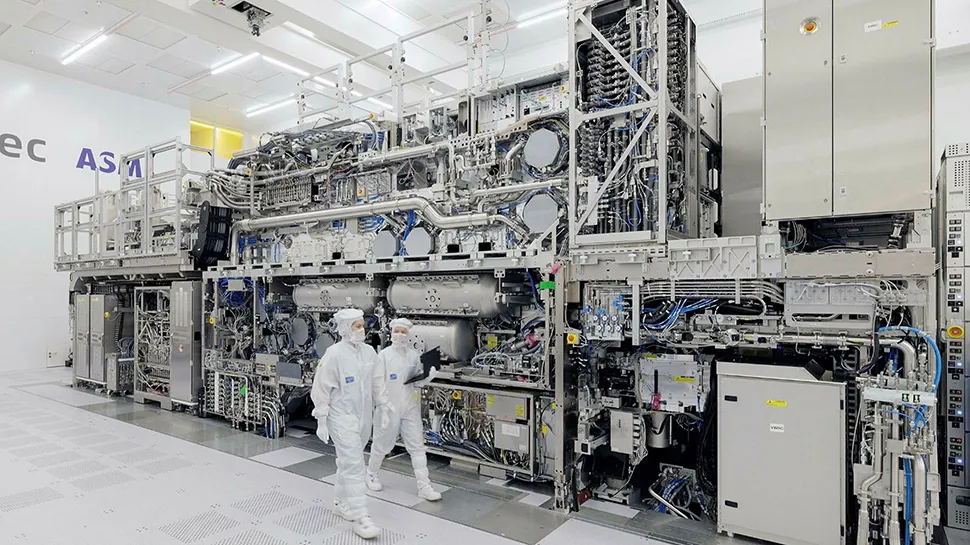
This system, which is around the size of a double decker bus and weighs 150,000 kilograms, is capable of etching lines just 8nm wide on semiconductors. This is a significant reduction from the previous generation, allowing for more transistors to be packed onto a chip, leading to faster processing and higher storage capacity, critical for AI applications.
Intel, a major customer, has already received its first machine at its D1X factory in Oregon and plans to commence production using the system by the end of 2025.
Not for China
“Intel’s focus is to stay at the forefront of semiconductor lithography technology and we’ve been building our EUV expertise and capacity over the last year. Working closely with ASML, we will harness High-NA EUV’s high-resolution patterning as one of the ways we continue Moore’s Law and maintain our strong history of progression down to the smallest of geometries,” said Dr. Ann Kelleher, executive vice president and general manager of Technology Development at Intel.
ASML says it taken between 10 and 20 orders to date of its machine, which is priced at a whopping $350 million, indicating optimistic expectations for the technology. This comes despite accusations concerning the cost-effectiveness of the next-generation lithography tool for upcoming nodes.
Although China was ASML's second-largest market last year, Reuters reports the new device won’t be sold to manufacturers there, following the United States government’s crack down on the export of cutting edge technology to the People's Republic.
EUV lithography, unique to ASML, prints microchips using light with a wavelength of just 13.5 nm – almost x-ray range. ASML (and Intel) say technology is driving Moore's Law forward and supporting novel transistor designs and chip architectures.
The new platform is expected to support high-volume chip manufacturing in 2025–2026, enabling geometric chip scaling into the next decade. By reducing the number of process steps in high-volume manufacturing, chipmakers could benefit from significant reductions in defects, cost, and cycle time.
More from TechRadar Pro
