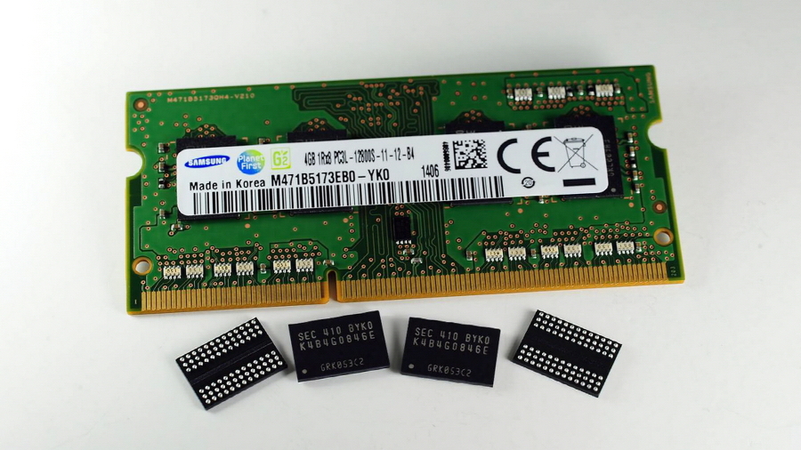
Samsung begins 20nm DRAM mass production
A chip off the old block

Sign up for breaking news, reviews, opinion, top tech deals, and more.
You are now subscribed
Your newsletter sign-up was successful
Join the club
Get full access to premium articles, exclusive features and a growing list of member rewards.
Samsung has begun mass production of new DDR3 memory chips using 20nm process technology, which it claims is the most advanced DRAM of its kind.
The 4GB chips employ a new scaling technology that uses modified double patterning and atomic layer deposition. Samsung had to use this approach to overcome scaling limits with DRAM compared to NAND Flash.
Samsung also improved its manufacturing productivity by switching to 20nm DDR3. Productivity is up by 30 per cent compared to 25nm chips and more than twice as much compared to 30nm designs.
Article continues belowEnergy-efficient
The smaller process technology is good for the environment too, with Samsung touting a 25 per cent reduction in energy consumption compared to previous memory chips.
"Samsung's new energy-efficient 20-nanometer DDR3 DRAM will rapidly expand its market base throughout the IT industry including the PC and mobile markets, quickly moving to mainstream status," said Young-Hyun Jun, executive VP of memory sales and marketing at Samsung.
Samsung's new modified double patterning technology also sets the stage for production of 10nm DRAM in the future, effectively future-proofing its investment in this area.
With revenue in the global DRAM market expected to grow to $37.9 billion (£22.8 billion, AU$41.9 billion) this year, according to Gartner, Samsung is well placed to cash in on its growing memory portfolio.
Sign up to the TechRadar Pro newsletter to get all the top news, opinion, features and guidance your business needs to succeed!
 Become a TechRadar Insider


