New chip tech 'biggest change in 40 years'
Intel shrinks transistors still further

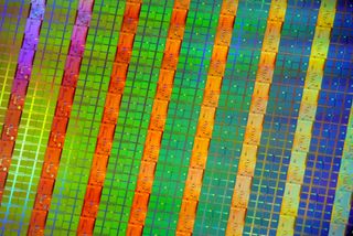
Intel has hailed its latest manufacturing process as the biggest change to chips in 40 years. The new 45nm process will ensure that quad and octo-core processing can become a reality on chips that are power and heat efficient.
The chip giant has said it is using "dramatically new materials" to build the insulating walls and switching gates for the new processors.
Intel will use a new material that has a property called high-k for the transistor gate dielectric, and a new combination of metal materials for the transistor gate electrode. These might not sound terribly exciting, but they are crucial parts of the chip.
The gate turns the transistor on and off, and the gate dielectric is an insulator underneath it that separates it from the channel where current flows. "The combination of the metal gates and the high-k gate dielectric leads to transistors with very low current leakage and record high performance," says Intel.
Chips in the pipeline
The company says it has five early version 45nm chips running with 15 processors in the pipeline for release. It seems these will continue to have the same Core and Xeon branding as before. The first family of processors are codenamed Penryn.
"The implementation of high-k and metal materials marks the biggest change in transistor technology since the introduction of polysilicon transistors in the late 1960s," said Intel's co-founder Gordon Moore. Moore was responsible for the peerless Moore's Law, which states that processing power doubles every two years. This is set to hold true into the next generation of processors as a result of the new manufacturing process.
Silicon dioxide has traditionally been used to make the transistor gate dielectric. Intel shrunk the silicon dioxide gate to as little as 1.2nm thick with its previous 65nm process technology, but the shrinking led to an increase in wasted electric current and unnecessary heat.
Get daily insight, inspiration and deals in your inbox
Get the hottest deals available in your inbox plus news, reviews, opinion, analysis and more from the TechRadar team.
A decade ago, the revered process technology was 250nm. Transistor dimensions were approximately 5.5 times the size, and 30 times the area, of those made using 45nm technology.
Contributor
Dan (Twitter, Google+) is TechRadar's Former Deputy Editor and is now in charge at our sister site T3.com. Covering all things computing, internet and mobile he's a seasoned regular at major tech shows such as CES, IFA and Mobile World Congress. Dan has also been a tech expert for many outlets including BBC Radio 4, 5Live and the World Service, The Sun and ITV News.
