
 Become a TechRadar Insider


Big news. The IBM Technology Alliance has announced its 28nm process and the first chips should be rolling off the lines by 2010 with ARM systems-on-a-chip (SoC) among the first. Are you excited? Yes? No? At the very least you should be impressed.
Despite endless predictions of insurmountable technical hurdles the semiconductor business has continued to trace Moore's predictions and are now rapidly heading towards the weird world of nanoelectronics.
Small is good
Using a smaller nanometre process is a Very Good Thing. It means lower power consumption, higher potential frequencies and, of course, more transistors, all good stuff.
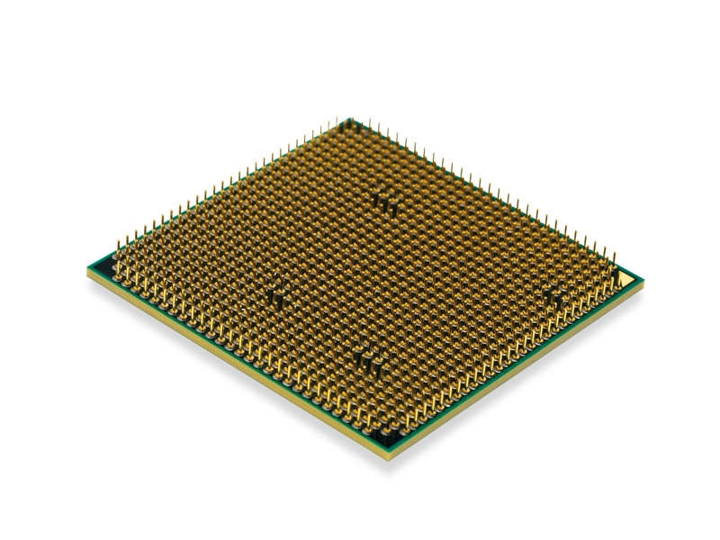
The best of AMD and Intel's processors currently use a 45nm process and Intel announced its 32nm Westmere processors in February for delivery before the end of the year. AMD currently seems to be about a year behind Intel, which makes IBM's announcement impressive stuff.
Semiconductors are created using photolithography, the design etched in light and chemically processed, simply rinse and repeat until you've built your chip up in layers. The trick to shrinking the design is getting an accurate beam onto your wafer and it is this process that has largely been the focus of the boffins, along with improved dielectric materials to stop electrons getting ideas of their own and wandering off track.
193nm lasers
The current tool of choice for tracing out your transistors is an argon-flouride deep ultraviolet excimer laser with a 193nm wavelength (mmmm nice). Now, how can you possibly make a 32nm process chip using a laser beam 193nm wide I hear you ask? Surely this is like using a JCB for weeding your borders? Two key technologies have recently emerged.
First, there's double patterning. In its simplest form this process uses two exposures, offset slightly to create features smaller than either exposure could create alone, effectively increasing the resolution by a factor of two.
You don't have to stop there either, triple and quadruple patterning is possible. Second, we have a process called immersion lithography, where the beam is shone thorough a liquid, this deflects and slows the beam and effectively gives you a resolution increase equal to the refractive index of the liquid, for water this is 1.44. Research into new liquids with refractive indices of 1.7 or more will increase the further.
Intel's Westmere employs immersion lithography on 'critical' layers. Combine these methods and you've turned your relatively clumsy beam into something much more accurate without any major changes in technology and, more importantly, completely rebuilding ridiculously expensive fabs.
The limits of photolithography have been announced as nearly reached many times, beyond one micron was once thought impossible, and yet each time the white-coated ones manage to squeeze higher resolutions out of it.
Why not just use a finer beam in the first place? An obvious solution and a lot of hard cash has been spent trying it, including using X-rays and focused ion and electron beams. Intel had high hopes for the 157nm laser, but problems with building suitable lenses have scuppered it for the time being.
One current front runner is the extreme ultraviolet laser with a wavelength of 13.5nm. So far though the high-power beam has proved too much for the current materials, causing a lot of collateral damage.